商品描述
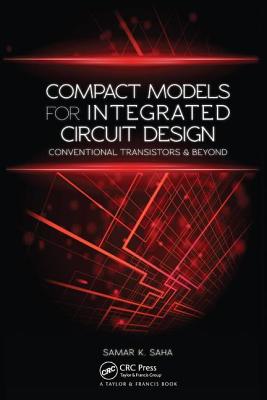
The text covers nanoscale semiconductor materials, device models, and applications for circuits design in a single volume. It will be a useful reference text for graduate students, and academic researchers in diverse areas such as electrical engineering, electronics and communication engineering, nanoscience and nanotechnology.
商品描述(中文翻譯)
本書涵蓋了納米尺度半導體材料、器件模型以及電路設計的應用,內容集中於單一卷冊中。這將成為電機工程、電子與通信工程、納米科學及納米技術等多個領域的研究生和學術研究者的重要參考書籍。
作者簡介
Dr. Balwinder Raj (MIEEE'2006) earned his B. Tech, Electronics Engineering (PTU Jalandhar), M. Tech-Microelectronics (PU Chandigarh) and Ph.D-VLSI Design (IIT Roorkee), India in 2004, 2006 and 2010 respectively. For further research work, European Commission awarded him "Erasmus Mundus" Mobility of Life research fellowship for postdoc research work at University of Rome, Tor Vergata, Italy in 2010-2011. Dr. Raj received India4EU (India for European Commission) Fellowship and worked as visiting researcher at KTH University, Stockholm, Sweden, Oct-Nov 2013. He also visited Aalto University Finland as visiting researcher during June 2017.Currently, he is working as Associate Professor at National Institute of Technical Teachers Training and Research Chandigarh, India since Dec 2019. Earlier, he was worked at National Institute of Technology (NIT Jalandhar), Punjab, India from May 2012 to Dec 2019. Dr. Raj also worked as Assistant Professor at ABV-IIITM Gwalior (An autonomous institute established by Ministry of HRD, Govt. of India) July 2011 to April 2012. He received Best Teacher Award from Indian Society for Technical Education (ISTE) New Delhi in 26th July 2013. Dr. Raj received Young Scientist Award from Punjab Academy of Sciences during 18th Punjab Science Congress held on 9th Feb 2015. He also received a research paper award in an international conference on Electrical and Electronics Engineering held at Pattaya, Thailand from 11th to 12th July 2015. Dr. Raj has authored/co-authored 3 books, 8 book chapters and more than 70 research papers in peer reviewed international/national journals and conferences. His areas of interest in research are Classical/Non-Classical Nanoscale Semiconductor Device Modeling; Nanoelectronic and their applications in hardware security, sensors and circuit design, FinFET based Memory design, Low Power VLSI Design, Digital/Analog VLSI Design and FPGA implementation.
Dr Ashish Raman earned his B.E, Electronics and Communication Engineering, M. Tech-Microelectronics and VLSI Design (Shri G S Institute of Technology and Science, Indore) and Ph.D-VLSI Design (NIT Jalandhar), India in 2003, 2005 and 2015 respectively. Currently, he is working as Assistant Professor at National Institute of Technology, Jalandhar, India since Sep 2007. Earlier, he was worked at National Institute of Technology (NIT Jalandhar), Durgapur, India from January 2007 to August 2007. Dr. Raman has authored/co-authored 1 book, 5 book chapters and more than 50 research papers in peer reviewed international/national journals and conferences. His areas of interest in research are VLSI Circuit Design, Nanoscale Semiconductor Device; Nanoelectronic, Modeling, Low Power VLSI Design, Digital/Analog VLSI Design and FPGA implementation, Sensor and circuit applications. He is working as principal investigator of various funded projects such as SMDP-C2SD sponsored by MeitY, FIST Sponsored by DST, FPGA based High Speed CCSDS Processor for Baseband Receiver, Funded by ISRO Banglore, and many more projects. Dr. Raman is a member of the IEEE Electron Devices Society, the IEEE Solid-State Circuits Society, and the Institution of Engineers Society, India
作者簡介(中文翻譯)
巴爾溫德·拉吉博士(MIEEE'2006)於2004年、2006年和2010年分別獲得印度PTU賈蘭達爾電子工程學士學位、PU昌迪加爾微電子碩士學位及IIT魯爾基VLSI設計博士學位。為了進一步的研究工作,歐洲委員會於2010-2011年授予他「Erasmus Mundus」流動生活研究獎學金,以進行在意大利羅馬托爾維爾加大學的博士後研究。拉吉博士於2013年10月至11月獲得India4EU(印度為歐洲委員會)獎學金,並在瑞典斯德哥爾摩的KTH大學擔任訪問研究員。他於2017年6月作為訪問研究員造訪芬蘭阿爾托大學。目前,他自2019年12月起在印度昌迪加爾國立技術教師培訓與研究所擔任副教授。此前,他於2012年5月至2019年12月在印度旁遮普的國立技術學院(NIT賈蘭達爾)工作。拉吉博士於2011年7月至2012年4月在ABV-IIITM瓜利奧爾(由印度人力資源發展部設立的自治機構)擔任助理教授。他於2013年7月26日獲得印度技術教育學會(ISTE)新德里的最佳教師獎。拉吉博士於2015年2月9日舉行的第18屆旁遮普科學大會上獲得旁遮普科學院的青年科學家獎。他還於2015年7月11日至12日在泰國芭堤雅舉行的國際電氣與電子工程會議上獲得研究論文獎。拉吉博士已著作或合著3本書、8章書籍及70篇以上的國際/國內期刊和會議的同行評審研究論文。他的研究興趣領域包括經典/非經典納米尺度半導體器件建模;納米電子學及其在硬體安全、傳感器和電路設計中的應用,基於FinFET的記憶體設計,低功耗VLSI設計,數位/類比VLSI設計及FPGA實現。
阿希什·拉曼博士於2003年、2005年和2015年分別獲得印度印多爾的Shri G S科技與科學學院電子與通信工程學士學位、微電子與VLSI設計碩士學位及NIT賈蘭達爾的VLSI設計博士學位。目前,他自2007年9月起在印度賈蘭達爾的國立技術學院擔任助理教授。此前,他於2007年1月至8月在印度杜爾卡普的國立技術學院(NIT賈蘭達爾)工作。拉曼博士已著作或合著1本書、5章書籍及50篇以上的國際/國內期刊和會議的同行評審研究論文。他的研究興趣領域包括VLSI電路設計、納米尺度半導體器件;納米電子學、建模、低功耗VLSI設計、數位/類比VLSI設計及FPGA實現、傳感器和電路應用。他擔任多個資助項目的主要研究員,如由MeitY贊助的SMDP-C2SD、由DST贊助的FIST、由ISRO班加羅爾資助的基於FPGA的高速CCSDS處理器等多個項目。拉曼博士是IEEE電子器件學會、IEEE固態電路學會及印度工程師學會的成員。


